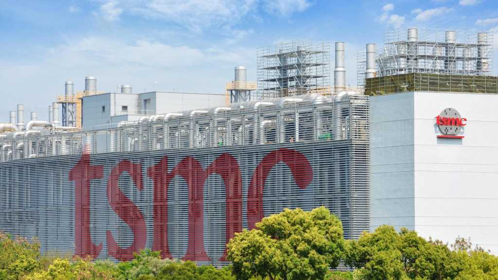
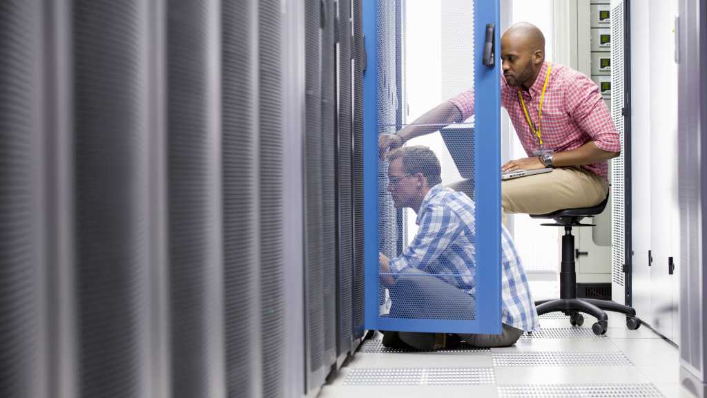
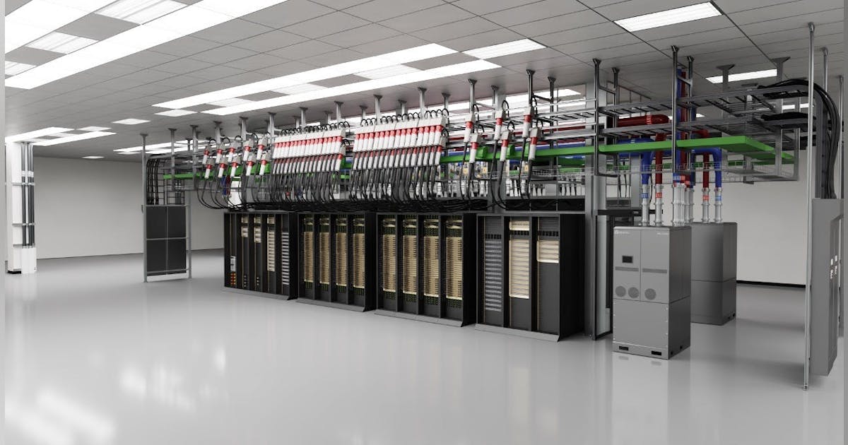
Nvidia’s flagship GPUs currently integrate two chips, while its forthcoming Rubin Ultra platform will connect four. “The SoW-X delivers wafer-scale compute performance and significantly boosts speed by integrating multiple advanced compute SoC dies, stacked HBM memory, and optical interconnects into a single package,” said Neil Shah, partner and co-founder at Counterpoint Research. “This approach reduces latency, improves power efficiency, and enhances scalability compared to traditional multi-chip setups — giving enterprises and hyperscalers AI servers capable of handling future workloads faster, more efficiently, and in a smaller footprint.” This not only boosts capex savings in the long run but also opex savings in terms of energy and space. “Wafer-X technology isn’t just about bigger chips — it’s a signal that the future of AI infrastructure is being redesigned at the silicon level,” said Abhivyakti Sengar, practice director at Everest Group. “By tightly integrating compute, memory, and optical interconnects within a single wafer-scale package, TSMC targets the core constraints of AI: bandwidth and energy. For hyperscale data centers and frontier model training, this could be a game-changer.” Priorities for enterprise customers For enterprises investing in custom AI silicon, choosing the right foundry partner goes beyond performance benchmarks. It’s about finding a balance between cutting-edge capabilities, flexibility, and cost. “First, enterprise buyers need to assess manufacturing process technologies (such as TSMC’s 3nm, 2nm, or Intel’s 18A) to determine if they meet AI chip performance and power requirements, along with customization capabilities,” said Galen Zeng, senior research manager for semiconductor research at IDC Asia Pacific. “Second, buyers should evaluate advanced packaging abilities; TSMC leads in 3D packaging and customized packaging solutions, suitable for highly integrated AI chips, while Intel has advantages in x86 architecture. Finally, buyers should assess pricing structures.”