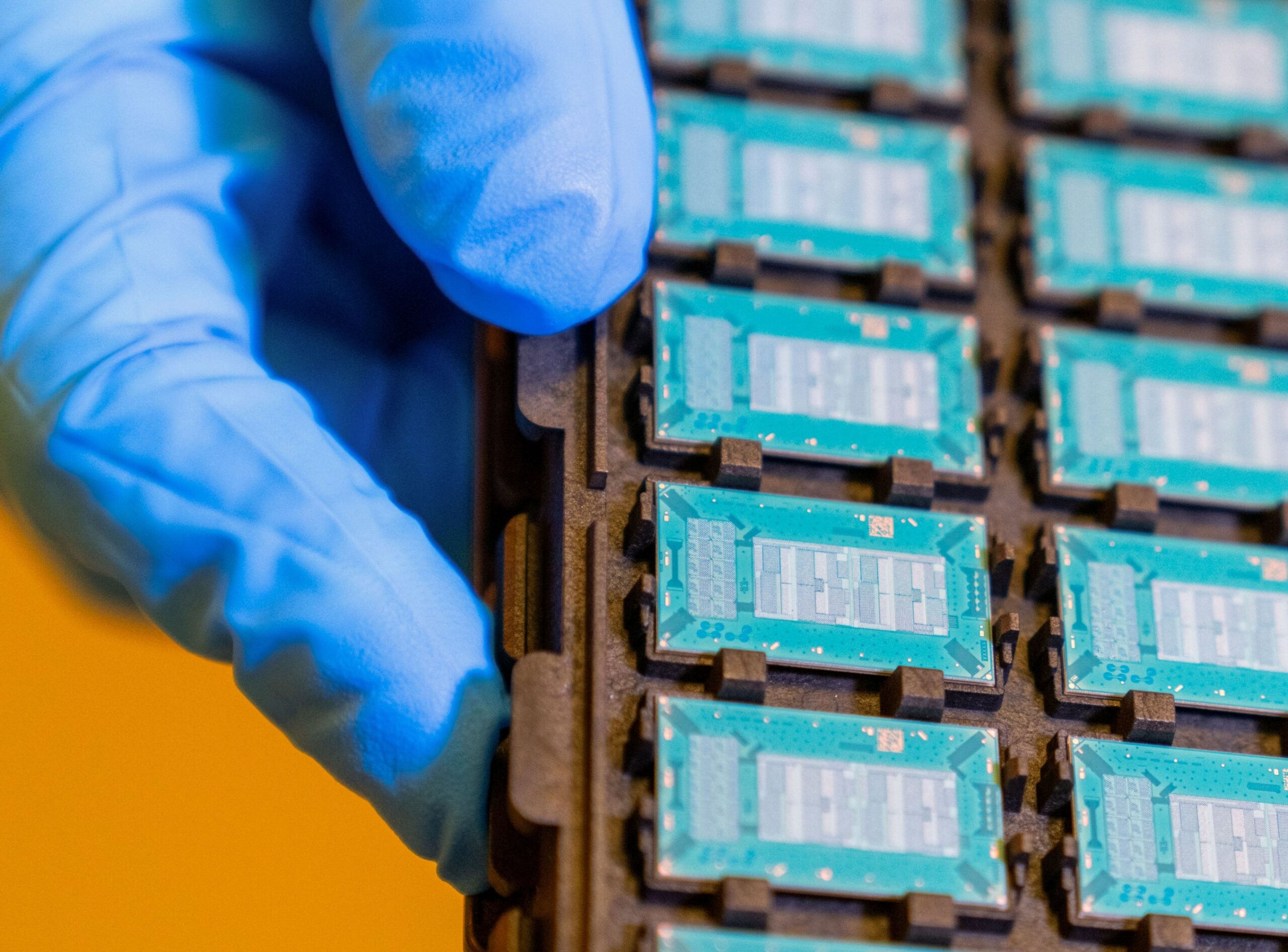
Silicon as a Data Center Design Tool
Custom silicon also allows hyperscale operators to shape the physical characteristics of the infrastructure around it.
Traditional GPU platforms often arrive with fixed power envelopes and thermal constraints. But internally designed accelerators allow companies like Meta to tailor chips to the rack-level power and cooling budgets of their own data center architecture.
That flexibility becomes increasingly important as AI infrastructure pushes power densities far beyond traditional enterprise deployments.
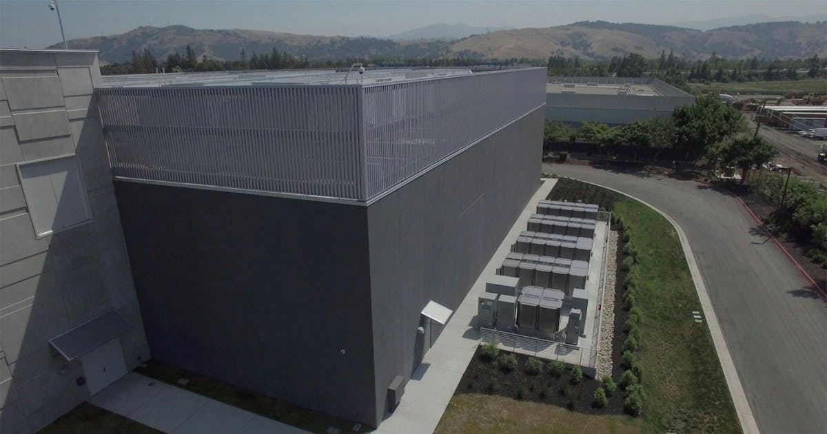
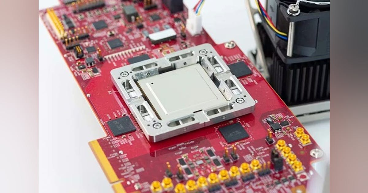
Custom accelerators like MTIA can be engineered to fit within the liquid-to-chip cooling frameworks now emerging in hyperscale AI racks.
These systems circulate coolant directly across cold plates attached to processors, removing heat far more efficiently than air cooling and enabling higher compute densities.
For operators running thousands of racks across multiple campuses, small improvements in performance-per-watt can translate into enormous reductions in total power demand.
Software-Defined Power
One of the subtler advantages of custom silicon lies in how it interacts with data center power systems.
By controlling chip-level power management features such as power capping and workload throttling, operators can fine-tune how servers consume electricity inside each rack.
This creates opportunities to safely run racks closer to their electrical limits without triggering breaker trips or thermal overloads.
In practice, that means data center operators can extract more useful compute from the same electrical infrastructure.
At hyperscale, where campuses may draw hundreds of megawatts, these efficiencies have a direct impact on capital planning and grid interconnection requirements.
The Interconnect Layer
AI accelerators do not operate in isolation. Their effectiveness depends heavily on how they connect to memory, storage, and other compute nodes across the cluster.
Industry analysts expect next-generation inference platforms to rely increasingly on high-speed interconnect technologies such as CXL (Compute Express Link) and advanced networking fabrics to support disaggregated memory architectures and low-latency data movement.
These fabrics allow accelerators to access large shared memory pools or SSD arrays while maintaining the throughput needed for real-time inference.
For hyperscalers operating massive distributed AI systems, the chip is only one piece of a broader infrastructure puzzle.
Hyperscalers Redesigning the Stack
Meta’s MTIA roadmap fits into a broader trend across the hyperscale ecosystem.
Several large cloud and internet platforms are developing their own AI processors to complement traditional GPU infrastructure.
Examples include:
• Google’s Tensor Processing Units (TPUs)
• Amazon’s Trainium and Inferentia processors
• Microsoft’s Maia AI accelerators
These chips allow hyperscalers to tailor hardware to their workloads while reducing reliance on constrained GPU supply chains.
At the same time, companies continue to deploy large clusters of GPUs for training large language models and other frontier AI systems.
The result is a hybrid architecture combining:
• GPU training clusters
• custom inference accelerators
• high-bandwidth memory architectures
• advanced networking fabrics
• liquid-cooled rack designs
The Gigawatt Context
Meta’s silicon program also reflects the broader scale of infrastructure now required to support AI.
Hyperscalers are increasingly planning mega-campuses capable of supporting hundreds of megawatts of IT load, with some projects ultimately approaching gigawatt-scale power consumption.
In that environment, efficiency gains at the chip level can determine whether a campus requires 400 megawatts, or 500.
Custom silicon gives hyperscalers a new lever to control that equation.
As AI infrastructure continues expanding, the relationship between silicon and buildings will only grow tighter.
The data center was once a neutral container for computing hardware.
In the AI era, the hardware itself is increasingly shaping the building.